In general, when we need to verify whether a TVS has been damaged, it usually means the system has already experienced some abnormal behavior. A Transient Voltage Suppressor (TVS) is a highly efficient protection device in diode form. It is used to protect downstream ICs from unexpected overvoltage and overcurrent caused by ESD (Electrostatic Discharge) or EOS (Electrical Overstress) events.
Under normal conditions, the TVS is connected in parallel with the protected line, so it does not affect system operation. During design, the TVS remains in a reverse-biased blocking state, with extremely small leakage current. Electrically, it behaves as if a very large resistor (tens to hundreds of megaohms) is connected in parallel with the line. For easier understanding, it can even be considered equivalent to an open circuit.
However, the tolerance of a TVS has its limits. When the energy from ESD or EOS exceeds its specifications, the device may suffer varying degrees of damage. Generally, when the PN junction of the diode is destroyed, its equivalent impedance drops sharply while the leakage current increases significantly. Therefore, in most cases, a damaged TVS presents itself as a short-circuit condition.
There is another possible failure mode where the TVS becomes open-circuit. This occurs when extremely high energy exceeding the device rating burns out the internal bonding wire. However, this situation is relatively rare. Moreover, if a damaged TVS becomes open-circuit, it typically does not affect system operation, so it may go unnoticed.
When abnormal system behavior is detected, the first step is usually to check both hardware and software. Once the issue is identified as related to a specific hardware function or circuit path, individual components must be analyzed. As shown in Figure 1, if the circuit exhibits reduced impedance or abnormal short-circuit behavior, components such as R, C, and TVS need to be examined.
Resistors (R) can be measured with a multimeter to check their resistance value. Parallel capacitors (C) can be tested to see whether they are shorted, and some multimeters with extended functions can also measure capacitance. Another method is the elimination method, where components are removed or replaced one by one for testing. Once the TVS component is removed from the circuit, the following three-step approach can be used to verify whether the TVS is damaged.

Figure 1. Circuit Troubleshooting
1. DC Electrical Test
A DC electrical test is the preliminary method to determine whether a TVS is functioning properly. The main parameters examined are breakdown voltage and leakage current.
A multimeter can provide a basic check:
•For a unidirectional TVS, the diode test function can be used.
The typical forward conduction voltage of a silicon diode is 0.6 V to 0.9 V.
•For a bidirectional TVS, the resistance mode can be used to see whether the impedance has dropped significantly or indicates a short circuit.
However, a multimeter can only provide a basic check for shorted TVS devices. The most important parameters—breakdown voltage and leakage current—require measurement with specialized equipment.
A common instrument is an I-V curve measurement system. As shown in Figures 2 and 3, Keysight’s I-V measurement equipment was used to measure the I-V curves of two suspected faulty devices, TVS(a) and TVS(b).
•The purple curve represents the normal I-V characteristic.
•The blue curve represents the measured results. For TVS(a), the measured I-V curve indicates a short-circuit condition, so it is classified as fail.
For TVS(b), although it does not show a short-circuit state, its leakage current exceeds the maximum specification limit, and therefore it is also classified as fail.

Figure 2. I–V Curve of TVS(a)

Figure 3. I–V Curve of TVS(b)
2. X-Ray Inspection
After electrical measurements, we can already determine whether the TVS is defective based on electrical parameters. However, if we want to further investigate the root cause of failure, additional analysis is required.
The second step is X-ray inspection, which is a non-destructive method used to observe the internal structure of the TVS.
In most TVS packages (except CSP packages), there are bonding wires inside the device. Therefore, one of the key purposes of X-ray inspection is to check whether these bonding wires are damaged.
In Figure 4, the X-ray image of TVS(a) clearly shows that the bonding wire has melted and broken (highlighted in the red box). Bonding wires are typically made of gold or copper. When they melt, it indicates that the TVS experienced energy far exceeding its rated capacity, resulting in severe damage.
In contrast, the X-ray result of TVS(b) in Figure 5 shows no obvious damage to the bonding wires or frame structure. Combined with the earlier I-V measurement showing only a slight increase in leakage current, this suggests that the device experienced relatively minor energy stress.
To confirm this preliminary conclusion, the third and most important step is required: Decapsulation (Decap).
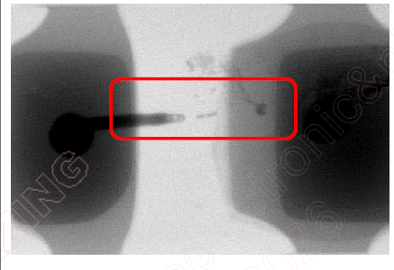
Figure 4. X-ray Image of TVS(a)

Figure 5. X-ray Image of TVS(b)
3. Decapsulation (Decap)
Decapsulation involves using chemical solvents to remove the package and then examining the die surface under a high-magnification microscope.
For TVS devices, EOS damage usually begins when excessive external energy breaks down the silicon semiconductor structure. As the EOS energy passes through the die, it may leave burn marks or carbonized traces, which reflect the magnitude of the energy involved.
For multi-channel TVS devices, the location of the burn marks can also help determine which pin introduced the destructive energy.
As shown in Figure 6, the die surface of TVS(a) shows large-area carbonization damage. This type of damage typically results from severe EOS energy, which also explains the previously observed melted bonding wire in the X-ray image.
Therefore, TVS(a) can be concluded to have been damaged by EOS.
In theory, a melted bonding wire should produce an open-circuit condition. However, in this case the severe burning caused carbonization and adhesion of conductive materials, so the I-V measurement still showed a short-circuit behavior.
Figure 7 shows the Decap result of TVS(b). A small burn mark can be observed on the die surface (red box), indicating that it experienced a relatively small EOS energy event. This aligns with the I-V test result, which showed only a slight increase in leakage current, and the X-ray inspection showing no structural damage to the bonding wires.
Another possible scenario is when the Decap result shows no visible surface damage on the die. In such cases, the damage may exist inside the die, which can occur with ESD events. ESD energy is typically much lower than EOS energy, so surface damage may not be visible.

Figure 6. Decap Image of TVS(a)

Figure 7. Decap Image of TVS(b)
The three-step approach—DC electrical testing, X-ray inspection, and Decapsulation—provides a systematic and comprehensive method for verifying whether a TVS device has failed.
This approach allows engineers to quickly and accurately determine the failure condition of defective components. Once the analysis results are obtained, it becomes possible to identify the source, type, and magnitude of the abnormal energy event, which helps guide improvements and countermeasures at the system level.
TVS devices are passive components, and they do not fail spontaneously without external energy triggering the damage. If the system cannot avoid exposure to abnormal energy events, one possible solution is to upgrade the TVS specifications. This can improve the energy tolerance of the TVS and strengthen the overall protection capability of the system.