With the continuous improvement of image quality, the higher resolution images require the larger storage space in cellphones or cameras. The increasing demand for better data transmission also leads to the need for higher transmission speed. Now, USB4 published by USB-IF, supporting 40 Gbit/s throughput, will be able to meet growing consumer demand for faster transmission rate. In order to reach higher effective transfer speed, the USB4 controller must be made by the advanced semiconductor manufacturing technology. However, it also leads to a significant reduction in ESD tolerance.
USB4 is built into the physical interface of USB Type-C. In addition to improve the maximum data rate to 40 Gbit/s, the USB-C PD can quickly charge devices with up to 100W of power. In the near future, USB Type-C will rapidly become a mainstream interface in most consumer electronics such as desktops, notebooks, tablets and smartphones.
Just like traditional USBs, USB4 port is visible and the user can freely connect and disconnect device to the system. The most common application is plug-and-play. However, the hot swap action is usually the cause of blowing electronic system up, or even results in the damage of USB Type-C controller, because such events may contribute to unwanted noise transients such as ESD. In hot swapping, the live signal line as charged wire at the interface port will discharge while making contact with the system. This kind of discharge (normally called “direct discharge”) triggered by hot swapping is same as electrostatic discharge which can seriously damage the system. In the system-level ESD testing, more and more manufacturers are requesting to perform Direct-Pin Injection to test their products (as shown in Figure 1) in order to simulate end-user ESD events that frequently occur in the real world.

Figure 1: Direct-Pin Injection testing setup
In terms of the system-level ESD testing, some brand manufacturers even specify that USB Type-C connectors installed on their products shall be tested by Direct-Pin Injection to pass ESD strikes for ±8kV contact discharge in addition to the IEC 61000-4-2 standard. Therefore, the use of ESD protection on USB Type-C interface is absolutely necessary to prevent ESD-induced interference on data transmission.
Electronic products have rapidly reached all corners of the world. However, weak infrastructure and extreme weather events in many areas increase the likelihood of damage to electronic devices caused by EOS (Electrical Over Stress) power surge, resulting in a significant increase in reported returns. IEC 61000-4-5 has been adopted for use as international test standard to simulate EOS events induced by power interference, noise on power lines or hot swapping, with voltage waveform of 1.2/50μs and current waveform of 8/20μs. In addition to performing Direct-Pin Injection as internal ESD test method, some brand manufacturers also include Direct-Pin Injection method for EOS test (as shown in Figure 2).

Figure 2: Direct-Pin Injection testing setup for EOS test
For a high-speed interface like USB4, there are some points that need to be taken into account for the selection of ESD/EOS protection component:
1. To assure the delivery of high-speed signal integrity through USB4, an ESD protection component with lower parasitic capacitance is required for the selection. Parasitic capacitance lower than 0.2pF is more recommended.
2. Choose a protection component that has a high ESD-tolerant voltage capability, at least to withstand over ESD strikes for 8kV contact discharge specified in IEC 61000-4-2.
3. ESD clamping voltage is an essential parameter. A lower clamping voltage indicates better protection performance. It means that the ESD energy is clamped to a lower voltage to prevent interference or damage to a system’s internal circuit. That makes the clamping voltage become the most important parameter to qualify the efficiency of an ESD protection component.
4. The charging technology of USB PD supports four voltage levels at 5V, 9V, 15V and 20V. However, frequent hot swapping to power supply can easily cause ESD/EOS events, and it is necessary to optimize ESD/EOS protection solution against external surges.
Amazing Microelectronic Corp. has advanced technology for ESD protection design, and released AZ5B9S-01F especially for USB4. To avoid parasitic capacitance from limiting the transmission of differential signal on USB4, the parasitic capacitance of AZ5B9S-01F is lower than 0.2pF to successfully pass Eye Diagram test at 40 Gbit/s. The best part is that AZ5B9S-01F has an extremely low ESD clamping voltage, which is able to effectively assist USB 4 interface to survive the ±8kV ESD strikes (contact discharge) in Direct-Pin Injection testing. The current-voltage curve of AZ5B9S-01F measured by TLP (as shown in Figure 3) indicates that the clamping voltage is only 4.6V under ESD strikes for 8kV contact discharge specified in IEC 61000-4-2 (with equivalent TLP current of approximately 16A), which can effectively avoid data errors, system crashes or even severe damages to system during ESD testing.
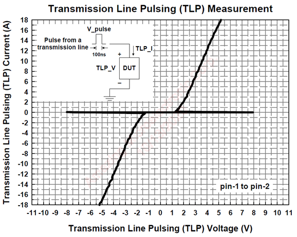
Figure 3: I-V characteristic curve of AZ5B9S-01F specifying ESD clamping performance
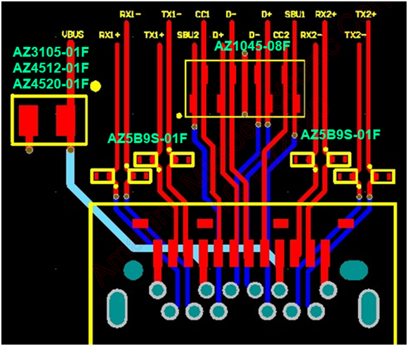
With the development trends of lighter, thinner and smaller electronic products, the printed circuit boards (PCBs) also keep getting smaller. Under the requirements of powerful functions, the circuit layout has become more complex and difficult on a tiny PCB, and increases product design challenges. The AZ5B9S-01F with ultra-small package DFN0603P2Y has a size of only 0.6mm x 0.3mm and a height of 0.3mm to mainly protect the 4 differential pairs (TX and RX) on USB4. Moreover, the use of single one AZ1045-08F is capable to protect the remaining signal lines (D+/D-/CC/SBU). In particular, the pins of AZ1045-08F are configured as staggered arrangement to facilitate the feed through design on PCB layout, which can avoid difficulties in wiring. It not only accelerates the PCB layout design process during design stage, but also minimize PCB size to reduce the costs of system. This interface also provides fast charging. The engineers may only need to select a suitable EOS component from AZ3105-01F, AZ4512-01F or AZ4520-01F at the power port as protection to perfectly protect the interface from ESD/EOS events. Figure 4 shows the ESD/EOS protection solutions for a complete wiring of USB4 interface.